 |
 |
 |
 |
 |
 |
|
Small Signal Amplifier SimulationWe've seen how the front end of the receiver comes together, so we can begin to look at simulating it. It's probably not necassary, but it will give us confidence that we're on the right path. Let's take a look at the test harness for the small signal amplifier we've been working on. 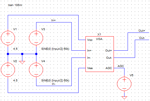
That's all there is to it! There are a couple of voltage sources to provide the supply rails, and another couple to generate a representaton of the signal from the antenna. You may have noticed that there are no bias resistors present at the front end. This is essentially because the stimulus voltage sources are referenced to ground. When we couple the antenna coil, it'll be different. The only thing in that circuit will be the antenna coil it's self, so we'll need to remember to include the bias networks on the schamatic for the PCB. The antenna signal sources are configured to generate a 60kHz signal of amplitude half the "Input" parameter. That's not on the schematic yet, but using a parameter allows us to change the size of the input signal in one place, and distribute it to the two voltage sources for the purposes of the simulation. It also means that we can express the magnitude of the balanced signal without having to think about it as being two halves of a signal. The voltage source on the AGC port is set to ramp from the negative supply rail to the positive supply rail, over the course of 100ms. You'll notice that I've named the important nodes so that they show up easily in the simulator results window. We'll run a transient analysis, and see what we get; 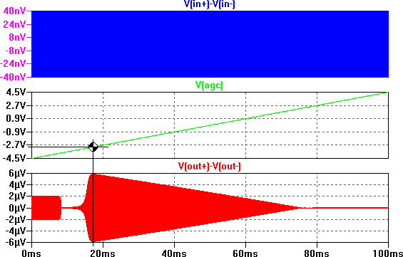
What we're looking at here, is a simulation with the input signal set to 80nV peak to peak. This is shown in blue at the top. We can't see the actual sine wave formation, but rest assured it's there. What we're interested in is the envelope. On the middle trace, in green, you can see the gain control input sweeping linearly between the supply rails. On the botttom trace you can see the output, in red, the combination of the input, and the varied gain. The round datum ball has been drawn in afterwards, sadly that kind of capability isn't available in spice! As we had thought, the useful range of the AGC control is clearly less than the supply rails. As much as it is unavoidable, this is actually good. In particular, we can see that the usable portion of the amplifier gain is nicely linear. This is the most important aspect. In detail the linear portion of the output is actualy rounded off where it approaches zero at the right hand end. It is from this rounding out that the logarithmic loop behaviour is derived. We'll see more of this later. I've drawn the datum ball on the simulation result, to show the AGC voltage which will yield maximum gain in the amplifier. In this case, with the smallest input signal we expect from the antenna, we're seeing a voltage gain of about 150 or 43dBV, which is more or less what we expect. Now, we'll push in the biggest signal that we think we'll see from the antenna, so we can make a comparison; 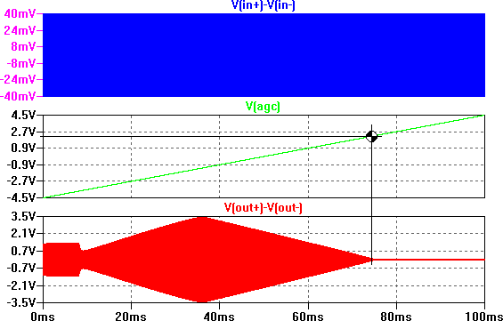
This time the graphs look slightly different. Although the basic plots and the AGC sweep are the same, the input is at 80mV peak to peak, a million times bigger or 120dBV. One of the important things to notice here is that the dynamic range of the AGC control is a fair bit bigger than the gain of the amplifier. That's important because it means that one variable gain amplifier is probably capable of doing the AGC control for all of the others. The more involved in controlling the gain, the more potential there is for loop noise to affect the final signal. This time we can see at the left of the graph, the region which was previously a good usable part of the linear range, is behaving oddly. What is happening here, is that the amplifier is well into distortion, or clipping. The load resistor and the supply rails limit the size of the output signal, and this interferes with the operation of the current sink. As time passes the reducing gain of the amplifier gradually brings the signal under control. At around 35ms into the simulation the amplifier enters the realm of linear control and perhaps, mild compression, due only to the non-linearities of the transistor. The important thing to take away, from this second simulation is the intercept on the far right of the slope in the output envelope. Now, with the big input signal, we can clearly see the low gain end of the operating range for the AGC control. With our range known, we can look at closing the loop. The diagram below shows some changes to the test harness; 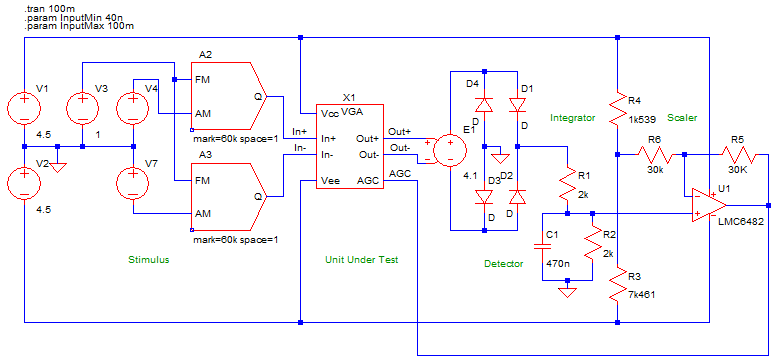
The harness has now moved on! We've tacked on some components that implement the upcoming receiver, in the simplest possible way. We've used ideal components explicitly. Ideally I would have chosen to describe the new part of the test harness purely mathematically, rather than through circuit components. The aim is to make the test harness as ideal as possible, such that the characteristics of the amplifier show up clearly. As it is SPICE will only allow parameters to be expressed mathematically. If you want to change voltages and currents during simulation with maths, rather than components you have to produce models, rather than circuits and sub circuits. The creation of models, is associated with significant effort. We can improvise satisfactorily with ideal components. So, what we're doing is buffering the output signal, and performing full wave rectification - mentioned previously. Then we integrate and scale to produce an AGC control signal. The integrator has been chosen to be quite fast. What we're aiming for here is to generate the actual envelope as a signal. In the final receiver, that will be too fast. Using the parameters from the previous simulation we can scale the signal, so that the logarithmic imapact on the gain of the system can clearly be seen. The basic aim, now that we have closed the loop is to vary the amplitude of the input signal linearly, and compare it with the amplitude of the output. This is the function of the of the sheet symbols A2 and A3. They are idealised components. They are voltage controlled oscillators with a frequency and an amplitude control. We fix the frequency at our usual 60kHz, but we control the range of the input signal between 40nV and 100mV peak, as the biggest concievable range of input signals. Using this scheme we can see the logging action. 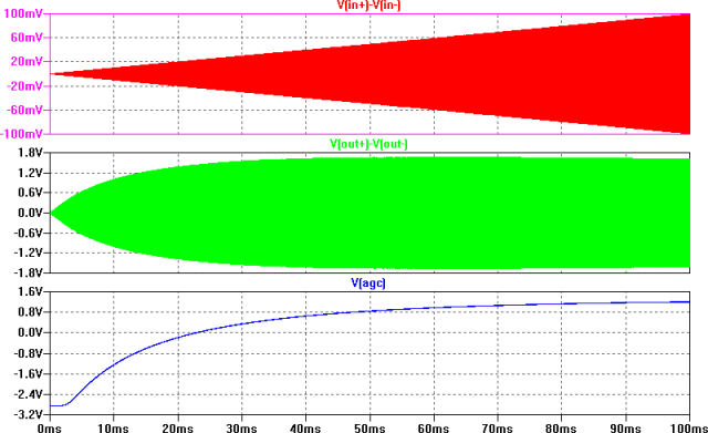
From the graph, the logging action is clear to see. What's interesting, is that to the right of the green output graph, the envelope of the signal seems to reduce slightly. The likelihood is that compression in the main amplifier transistors is getting the better of linearity in the signal path. What we can realise from this graph, is that there is a trade to be had between gain, and dynamic range. We have way more dynamic range than we need. When we finally tune the overall receiver, we'll be tuning for gain, not dynamic range. For the time being, we can be pretty satisfied with the performance of this "front end" small signal amplifier. By stacking similar amplifiers, we know that the others, in all probablility can be fixed gain. A slight variation in their flavour, will do away with some of the variable current source components. We can use a fixed current source, to get a fixed gain amplifier. By cascading these two flavours of the amplifier, we can get as much gain as we want to bring the tiny RF signal into the realm of the standard Op-Amp's we want to be using. Having looked at how to achieve sensitivity and dynamic range, we can now move on to look at a scheme to achieve selectivity. |


Copyright © Solid Fluid 2007-2025 |
Last modified: SolFlu Sat, 19 Nov 2011 01:40:46 GMT |