 |
 |
 |
 |
 |
 |
|
Small Signal Amplifier Design
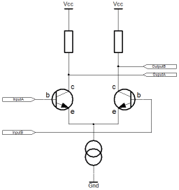
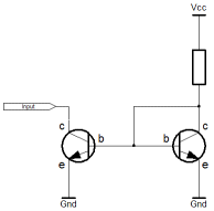
Previously, we looked at getting a stake in the ground. We covered the front end, and realised that the signal from the antenna would be pretty small. Too small in fact, for an op-amp to deal with in a reasonable way. Here we get down to the business of figuring out our main small signal amplifier. Once done, we'll use this amplifier in two different ways in the receiver design, and again in the test harness. We've already described that the coil antenna will be driving, a potentially long downlead. If we can, we want to provide the best possible rejection for signals that might couple into that downlead. Typically this leads to the use of a balanced line connected to the antenna coil. Since the coil is a current mode device, this idea works well (in theory) anyway. For the downlead we could either use twinaxial cable, or since we're dealing with a fairly low frequency, perhaps just a twisted pair. If we go with the balanced line, the front end amplifier of the receiver will have to be a differential amplifier. There, it's done! Differential AmplifierThe differential amplifier, sometimes known as a "long tail pair" is a fairly straightforward construct. Typically two NPN transistors (although not necassarily) are connected in a common emitter configuration. The collectors are connected to the power supply through similar load resistors, and the emitters are connected together and then down to ground through a current sink. The output of the amplifier is connected below each of the load resistors, where the potential (voltage) developed is controlled by the current through the resistor.
The base of each transistor is connected to each side of the balanced line. A positive going signal one one side of the input corresponds with a negative going signal on the other. Because the emitters of the two tansistors are connected together and feed into a current sink, only a differential input can affect the output. If an unwanted signal were to couple into the downlead, or the circuit, then it would be equally present on both sides of the balanced line; unable to affect the output of the amplifier. The basic assumption is that the current sink is always sinking the maximum current it is capable of. No matter what that current is, the only way a difference in potential at the output can occur is by one transistor tending off, and the other tending on. In addition to this "locking" of the two transistors together through their emitters (and the current sink) is a regenerative effect. Even though the inputs are intended to be opposites, if one input changes, and the other does not, it will cause the potential on the current sink to rise. We already stated that the sink is configured to be at it's maximum sink rate. Because the emitter potential rises, the base emitter junction voltage will reduce tending both transistors off. Since one of the transistors is more on than the other, it can be considered to have turned the other off. This regenerative effect is very important to the crisp behaviour of a differential amplifier. The signals that we'll be amplifying are very small. Unless we do something with them, they'll be isolated from the rest of the circuit. In order to turn the transistors of the differential amplifier on, we will need at least a diode drop of voltage on the base emitter junction. We don't have that from the antenna coil alone. We'll need to bias the inputs to the amplifier to set an operating point for these transistors and provide a quiescent current on the base. This ensures that the current sink is saturated. We can do it with a simple divider. The ratio of the divider should be arranged to split the supply rails more or less equally, but also such that in parallel the resistors constrain the quiescent base current to a reasonable level. Current Mirror
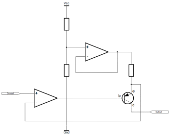
We've spoken about the differential amplifier, now we need to think about the current sink which is critical to its capability. The easiest way to achieve this sink, is to use a current mirror. A current mirror, like the differential amplifier is a simple construct. The basic idea of the current mirror is to provide a constant current sink or source, by setting a precise base emitter voltage on a sink or source transistor. Clearly it's pretty hard to do this with resistors. Although one can use resistors in series, and parallel, to achieve a virtually limitless range of values, the gain of transistors vary greatly with temperature. A current mirror circumvents this problem to some degree, by using another transistor to "calculate" the correct base emitter voltage for a given current sink capability. It's pretty simple. One uses a "programming" resistor from a suitable supply rail to set the current in the calculating transistor. The low side of the programming resistor is connected to the base of the sink transistor and both the base and collector of the calculating transistor. The emitters of both the sink and the calculating transistors are connected directly to a low side rail or ground. Because of this, it is easy to calculate the current in the programming resistor. Irrespective of the collector on the calculating transistor, all that is below the the progrmming resistor are the diode drops of the two transistors. We know they're going to be more or less on, so we can assume that this will be more or less a standard diode drop. Using Ohm's law it's easy to calculate the current from the rails and through the diode to a reasonable degree of precision. It's not that precise, but it can be tuned if necassary. Given that we've connected the base and the collector of the calculating transistor together, we can assume that the transistor will turn its self on, to the extent that the required current can be disposed of through the collector rather than the base, since the calculating transistor has gain. Most significantly, the base of the calculating transistor must have the correct potential to sink the program current. We can then distribute this potential to another transistor, the sink transistor, and know that it's base will have the correct potential to sink that same programming current. There are many ways in which this arrangement could be considered to introduce errors. It's hard to predict precisely, the voltage at the base of the calculating transistor, but this problem is not huge when compared with that of even precision resistors. Low gain transistors will obviously be less precise than high gain ones. Differences between the transistors will also introduce errors. All of these pale when considering the alternative, of setting up a divider on the base. Perhaps worse is the voltage dependence of a simple series resistor. Resistor values change far less with temperature, than the gains of transistors. A direct divider will show this clearly. The current mirror will be far more immune to such temperature dependence, because both transistors will be similarly temperate. The current mirror uses the natural tracking of the two transistors to compensate temperature, together with the programming resistor's comparative independence of temperature. One can also devise more advanced strategies where the programming resistor is fed from a variable voltage source. By varying the potential at the top of the programming resistor, one can vary the current in it. In our case we'll need this capability, it opens up the possibility of producing a variable current sink. Variable GainWhen thinking back to the system diagram, I drew the variable gain amplifier at the front of the receiver. This was for a specific reason. If we can achieve sufficient dynamic range by varying the gain of the first amplifier, then that is the only place we need to vary the gain. More, we should do it there. The sooner we get the variable gain element for the AGC out of the way the better. If we are receiving a small signal and the gain is high, we might suddenly receive a really big signal. If this were to happen, and the variable gain amplifier were some way down the chain, the front of the receiver might saturate. All further processing would be rendered useless. By placing the variable gain amplifier at the front, we help protect the receiver from becoming swamped. Looking back at the differential amplifier, and the current mirror, it is a fairly short step to produce a variable gain amplifier. I described how the differential amplifier worked, and the importance of the regenerative effect in the paired transistors. Critical to the operation of the differential amplifier is the potential of the node where the transistor emitters are tied to the current sink. By controlling the potential of this node, relative to the bias potential from the respective dividers on the bases, we can control the average current in the base emitter junction. Perhaps, another way to look at this is that any voltage developed across the collector load resistors are due the currents through them. Since the majority of that current pass through the sink, if we reduce the capacity of the sink, then the voltage developed across the load resistor must also reduce.
By changing the capacity of the current sink, we can change the gain of the amplifier. When I described the current mirror, I explained that we could vary it's capacity to sink, by adjusting the potential at the top of the programming resistor. What I actually implement is subtly different. In practice I use a variable current source. In the diagram, I show an arrangement where we use a couple of op-amps to control the programming current directly. By this very means we can build a voltage controlled variable gain amplifier. Perhaps one of the nicest features of such a scheme for variable gain, is that the minimum gain is limited to zero, and not one. If you remember I said that the potential of the common emitter and sink junction was important becuase it can control the base emitter junction potential relative to the base bias resistor network. This means that the minimum gain is zero. If the potential at the top of the sink is greater than that of the bias network on the base of the input transistors, they cannot conduct, or allow any curent through the load resistors. It's much better that we think in terms of the programming currents, than it is the turnoff voltage of the main amplifier transistors. Primarily this is because we want to control the sink current for maximum, and not minimum, gain. If we're thinking about maximum gain in terms of current in the sink, and minimum gain in terms of voltage on the sink node, we're in trouble. We must think about minimum gain in terms of zero current in the sink. The programming resistor is still present in the diagram, we just use a pass transistor to regulate the voltage on the low side. The buffer amplifier driving the programming resistor is important for causing it to be possible to turn off the current source completely. Op-Amps will rarely output to the rails, so we use a buffer amplifier on a divider to drive the programming resistor. This approach allows us to be able to "reach" the top of the programming resistor with the control amplifier output. Reaching though the pass transistor is critical to the overall logarithmic behaviour of the AGC loop. In simple terms when the setting for the current in the sink is big, the amplifier gain is big. By lowering the current in the sink, amplifier gain is reduced, and ultimately, when the current falls to zero so does the gain. This gives us a very powerful capability to limit the strength of big incoming signals. As long as the signals are not so large that they literally destroy the input transistors, we know that we can always reign them in by setting the front end gain to almost zero. When we close the AGC loop,it gives the receiver a logarithmic control over small gains, and that translates to good receiver dynamic range. So, if we can achieve the overall maximum voltage gain that we need, and we can get to "zero gain" should we need it, the dynamic range has more or less taken care of it's self. In practice there is still a large signal limit but it involves destroying the front end. That's unlikely, and we'll not revisit it. SimulationThe diagram below shows the complete circuit as simulated. Have a look and we can walk quickly through the simulation work which verifies our assumptions, and gives us some numbers that we can work with for other aspects of the receiver design. 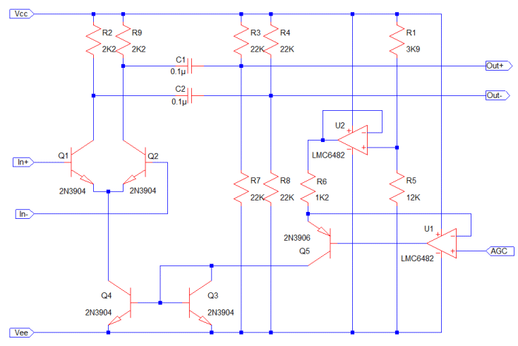
You'll probably notice that I've opted to use the LMC6482 op-amp for the variable current source, rather than the TL081. I alluded to the problem earlier when I mentioned that the problem of rail to rail outputs. The TL081 is a fairly old design, and this makes it good for a range of reasons, particularly it's combination of performance and cost. It's headroom requirements are really quite stringent, however. Typically if one far exceeds the input range specifications, the TL081 will exhibit "foldback". Instead of saturating at the maximum output value, the amplifier output will actually become the opposite of what one expects. This can lead to all manner of nasty or confusing conditions. The golden rule really, is that if one expects to operate within a couple of volts of the supply rails, one should be thinking about a "rail to rail" amplifier. Compared with the TL081 the LMC6482, is much more expensive, but it's modern accurate, and generally pretty well behaved. It doesn't quite have the bandwidth of the TL081 or the same power supply range but they're, broadly comparable. It's a modern general purpose op-amp, it's got a sensible head on it. In the old days chip designers were still smart but they used to drink petrol and read popular mechanics!!! Ill behaving op-amps have always been around, and will always be around (sometimes esoteric is good), but the LMC6482 is allright in my book! The circuit above, is formed about the subcircuits we've already seen. It's been drawn up In the Linear Technology SPICE program, which is superb for the price - free! The spice models for the transistors were both in the library that came with spice. The Spice model for the LMC6482 came direct from the National Semiconductor website. The help for the application fully describes how to integrate external spice models, but if you're already familiar with the way SPICE works you'll realise that nothing really has changed in years. It works, and well, why fix it! On the next page, we'll look at the actual simulation and results. |


Copyright © Solid Fluid 2007-2025 |
Last modified: SolFlu Sat, 19 Nov 2011 01:27:47 GMT |